LED lighting and Lasers are used in a variety of inspection systems in the semiconductor industry. Vision systems are used in wafer inspection systems to detect flaws, in measurement systems to identify inconsistencies in patterns, and in package inspection systems to check batch numbers and barcodes and to check the appearance of products. Reliable, high performance LED lights and lasers are critical to ensuring high quality inspection and maximizing throughput.
ProPhotonix LED lights and lasers are widely utilized to ensure quality in the semiconductor industry.

3D Measurement
3D measurement is often used in the semiconductor industry to measure the height of pastes and epoxies, and also to measure the flatness of wafers. 3D measurement can be used for inspection, sorting and defect detection.
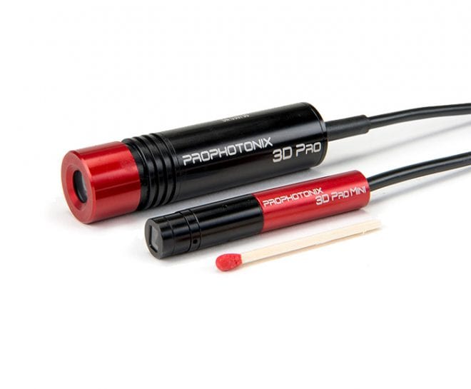
3D Pro Lasers
3D PRO lasers provide an ideal solution for 3D measurement applications in the semiconductor industry. These lasers offer excellent uniformity, with narrow line thickness and wide range of wavelengths and powers. Line widths down to 40µm at 120mm which is ideal for inspection applications that demand a high degree of accuracy. They also offer output powers up to 150mW and fan angles between 10° and 90°. Wavelengths range from 520nm to 850nm and include 635nm and 660nm.

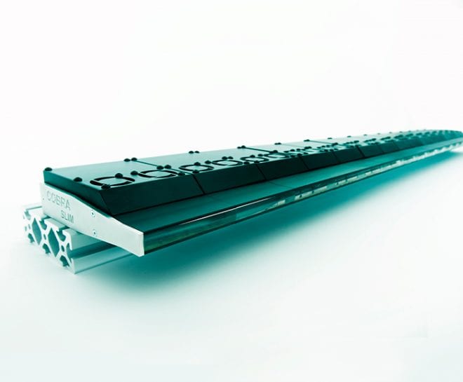
COBRA™ Slim LED Line Light
COBRA Slim is used in the semiconductor industry for 2D inspection of both wafers and PCBs. Wafers and PCBs are manufactured in various shapes and sizes, so a well illuminated target is essential for vision inspection. The COBRA Slim’s high uniformity is useful when inspecting reflective surfaces such as wafers and our IR COBRA Slim is useful for detecting defects within wafers. In the Electronics Industry, COBRA Slim is used to inspect PCBs and components.
Need help to optimize for your application?
For comprehensive technical support. Talk to us.
Contact UsContact Us
Bernhard Russell
Inside Sales

Andrea Gregorio
Inside Sales


